Æ
1/8
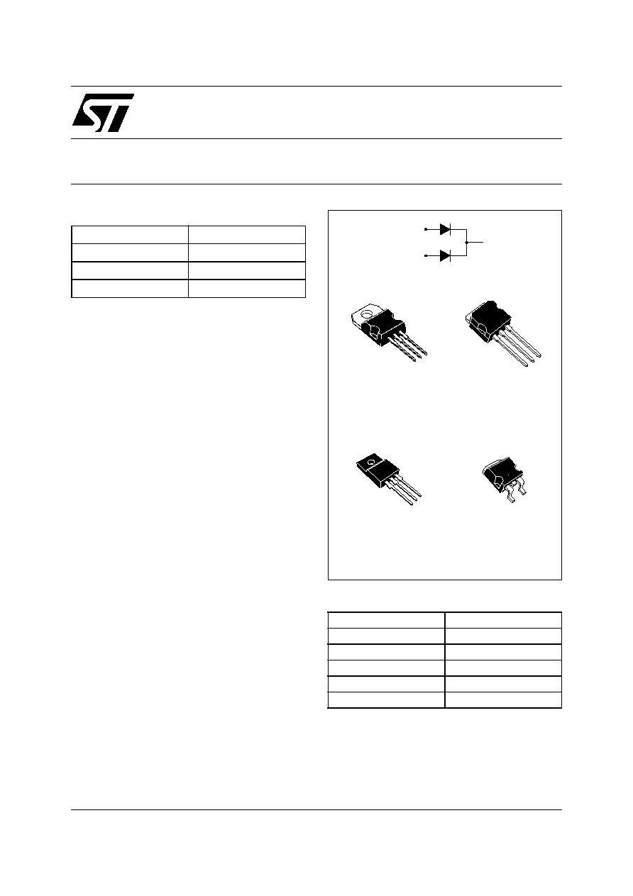
Table 1: Main Product Characteristics
I
F(AV)
2 x 10 A
V
RRM
45 V
T
j
(max)
175∞C
V
F
(typ)
0.57 V
STPS2045C
POWER SCHOTTKY RECTIFIER
REV. 5
A1
K
A2
A1
K
A2
TO-220AB
STPS2045CT
I
2
PAK
STPS2045CR
K
A1
A2
A1
K
A2
A1
A2
K
TO-220FPAB
STPS2045CFP
D
2
PAK
STPS2045CG
November 2004
FEATURES AND BENEFITS
Very small conduction losses
Negligible switching losses
Extremely fast switching
Insulated package: TO-220FPAB
Insulating voltage = 2000V DC
Capacitance = 12 pF
Avalanche rated
DESCRIPTION
Dual center tap Schottky rectifier suited for
SwitchMode Power Supply and high frequency
DC to DC converters.
Packaged either in TO-220AB, TO-220FPAB,
I
2
PAK, or D
2
PAK, this device is especially
intended for use in low voltage, high frequency
inverters, free wheeling and polarity protection
applications.
Table 2: Order Codes
Part Number
Marking
STPS2045CT
STPS2045CT
STPS2045CFP
STPS2045CFP
STPS2045CG
STPS2045CG
STPS2045CG-TR
STPS2045CG
STPS2045CR
STPS2045CR

STPS2045C
2/8
Table 3: Absolute Ratings (limiting values, per diode)
Table 4: Thermal Resistance Parameters
Table 5: Static Electrical Characteristics (per diode)
Pulse test:
* tp = 380 µs,
< 2%
To evaluate the conduction losses use the following equation: P = 0.42 x IF(AV) + 0.015 IF
2
(RMS)
Symbol
Parameter
Value
Unit
V
RRM
Repetitive peak reverse voltage
45
V
I
F(RMS)
RMS forward voltage
30
A
I
F(AV)
Average forward current
= 0.5
TO-220AB /
D
2
PAK / I
2
PAK
T
c
= 155∞C Per diode
10
A
TO-220FPAB
T
c
= 125∞C Per device
20
I
FSM
Surge non repetitive forward current
tp = 10ms sinusoidal
180
A
I
RRM
Repetitive peak reverse current
tp = 2µs F = 1kHz
square
1
A
I
RSM
Non repetitive peak reverse current
tp = 100ms square
2
A
P
ARM
Repetitive peak avalanche power
tp = 1µs Tj = 25∞C
4000
W
T
stg
Storage temperature range
-65 to + 175
∞C
T
j
Maximum operating junction temperature *
175
∞C
dV/dt
Critical rate of rise of reverse voltage
10000
V/µs
* :
thermal runaway condition for a diode on its own heatsink
Symbol
Parameter
Value
Unit
R
th(j-c)
Junction to case
TO-220AB / D
2
PAK / I
2
PAK Per diode
Total
2.2
1.3
∞C/W
TO-220FPAB
Per diode
Total
4.5
3.5
R
th(c)
Coupling
TO-220AB / D
2
PAK / I
2
PAK Coupling
0.3
∞C/W
TO-220FPAB
2.5
When the diodes 1 and 2 are used simultaneously:
Tj(diode 1) = P(diode 1) x Rth(j-c)(per diode) + P(diode 2) x Rth(c)
Symbol
Parameter
Tests conditions
Min.
Typ
Max.
Unit
I
R
*
Reverse leakage current
T
j
= 25∞C
V
R
= V
RRM
100
µA
T
j
= 125∞C
7
15
mA
V
F
*
Forward voltage drop
T
j
= 125∞C
I
F
= 10A
0.5
0.57
V
T
j
= 25∞C
I
F
= 20A
0.84
T
j
= 125∞C
0.65
0.72
dPtot
dTj
---------------
1
Rth j
a
≠
(
)
--------------------------
<
STPS2045C
3/8
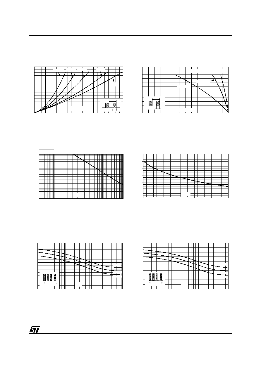
Figure 1: Average forward power dissipation
versus average forward current (per diode)
Figure 2: Average forward current versus
ambient temperature (
= 0.5, per diode)
Figure 3: Normalized avalanche power
derating versus pulse duration
Figure 4:
Normalized avalanche power
derating versus junction temperature
Figure 5: Non repetitive surge peak forward
current versus overload duration (maximum
values, per diode) (TO-220AB, D
2
PAK, I
2
PAK)
Figure 6: Non repetitive surge peak forward
current versus overload duration (maximum
values, per diode) (TO-220FPAB)
0
1
2
3
4
5
6
7
8
9
10
11
12
0
1
2
3
4
5
6
7
8
P
(W)
F(AV)
I
(A)
F(AV)
T
=tp/T
tp
= 1
= 0.5
= 0.2
= 0.1
= 0.05
I
(A)
F(AV)
0
25
50
75
100
125
150
175
0
2
4
6
8
10
12
TO-220AB
D≤PAK
TO-220FPAB
T
(∞C)
amb
T
=tp/T
tp
R
=R
th(j-a)
th(j-c)
R
=15∞C/W
th(j-a)
0.001
0.01
0.1
0.01
1
0.1
10
100
1000
1
t (µs)
p
P
(t )
P
(1µs)
ARM p
ARM
0
0.2
0.4
0.6
0.8
1
1.2
25
50
75
100
125
150
T (∞C)
j
P
(t )
P
(25∞C)
ARM p
ARM
1E-3
1E-2
1E-1
1E+0
0
20
40
60
80
100
120
140
I (A)
M
T =100∞C
C
T =125∞C
C
T =75∞C
C
t(s)
I
M
t
=0.5
1E-3
1E-2
1E-1
1E+0
0
20
40
60
80
100
I (A)
M
T =100∞C
C
T =125∞C
C
T =75∞C
C
t(s)
I
M
t
=0.5
STPS2045C
4/8
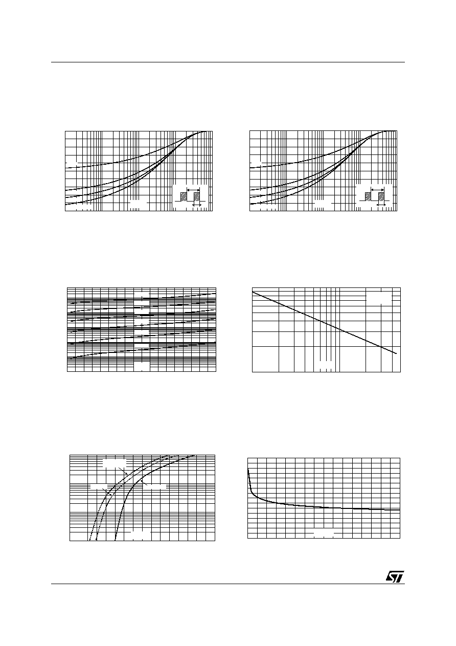
Figure 7: Relative variation of thermal
impedance junction to ambient versus pulse
duration (TO-220AB, D
2
PAK, I
2
PAK)
Figure 8: Relative variation of thermal
impedance junction to ambient versus pulse
duration (TO-220FPAB)
Figure 9: Reverse leakage current versus
reverse voltage applied (typical values, per
diode)
Figure 10: Junction capacitance versus
reverse voltage applied (typical values, per
diode)
Figure 11: Forward voltage drop versus
forward current (maximum values, per diode)
Figure 12: Thermal resistance junction to
ambient versus copper surface under tab
(Epoxy printed circuit board, copper
thickness: 35µm) (D
2
PAK)
1E-4
1E-3
1E-2
1E-1
1E+0
0.0
0.2
0.4
0.6
0.8
1.0
Single pulse
= 0.1
= 0.2
= 0.5
t (s)
p
Z
/R
th(j-c)
th(j-c)
T
=tp/T
tp
1E-3
1E-2
1E-1
1E+0
1E+1
0.0
0.2
0.4
0.6
0.8
1.0
Single pulse
= 0.1
= 0.2
= 0.5
t (s)
p
Z
/R
th(j-c)
th(j-c)
T
=tp/T
tp
0
5
10
15
20
25
30
35
40
45
1E-1
1E+0
1E+1
1E+2
1E+3
1E+4
5E+4
I (µA)
R
V (V)
R
T =150∞C
j
T =125∞C
j
T =100∞C
j
T =75∞C
j
T =50∞C
j
T =25∞C
j
1
2
5
10
20
50
100
200
500
1000
C(pF)
V (V)
R
F=1MHz
V
=30mV
T =25∞C
OSC
RMS
j
0.0
0.2
0.4
0.6
0.8
1.0
1.2
1.4
1.6
0.1
1.0
10.0
100.0
I
(A)
FM
T =125∞C
(typical values)
j
T =125∞C
j
T =25∞C
j
V
(V)
FM
0
5
10
15
20
25
30
35
40
0
10
20
30
40
50
60
70
80
S(cm≤)
R
(∞C/W)
th(j-a)
STPS2045C
5/8
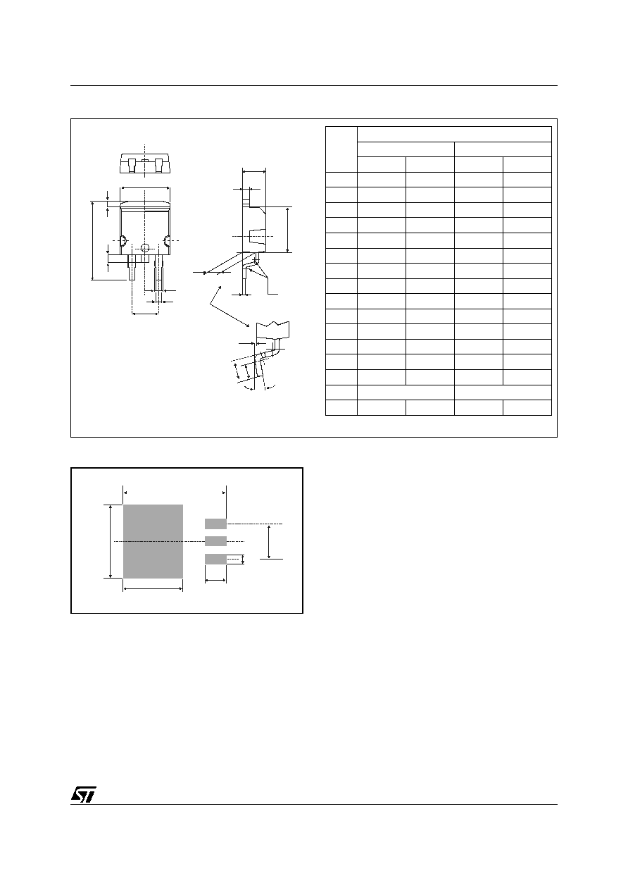
Figure 13: D
2
PAK Package Mechanical Data
Figure 14: Foot Print Dimensions (in millimeters)
G
L
L3
L2
B
B2
E
* FLAT ZONE NO LESS THAN 2mm
A
C2
D
R
A2
M
V2
C
A1
*
16.90
10.30
8.90
3.70
5.08
1.30
REF.
DIMENSIONS
Millimeters
Inches
Min.
Max.
Min.
Max.
A
4.40
4.60
0.173
0.181
A1
2.49
2.69
0.098
0.106
A2
0.03
0.23
0.001
0.009
B
0.70
0.93
0.027
0.037
B2
1.14
1.70
0.045
0.067
C
0.45
0.60
0.017
0.024
C2
1.23
1.36
0.048
0.054
D
8.95
9.35
0.352
0.368
E
10.00
10.40
0.393
0.409
G
4.88
5.28
0.192
0.208
L
15.00
15.85
0.590
0.624
L2
1.27
1.40
0.050
0.055
L3
1.40
1.75
0.055
0.069
M
2.40
3.20
0.094
0.126
R
0.40 typ.
0.016 typ.
V2
0∞
8∞
0∞
8∞
STPS2045C
6/8
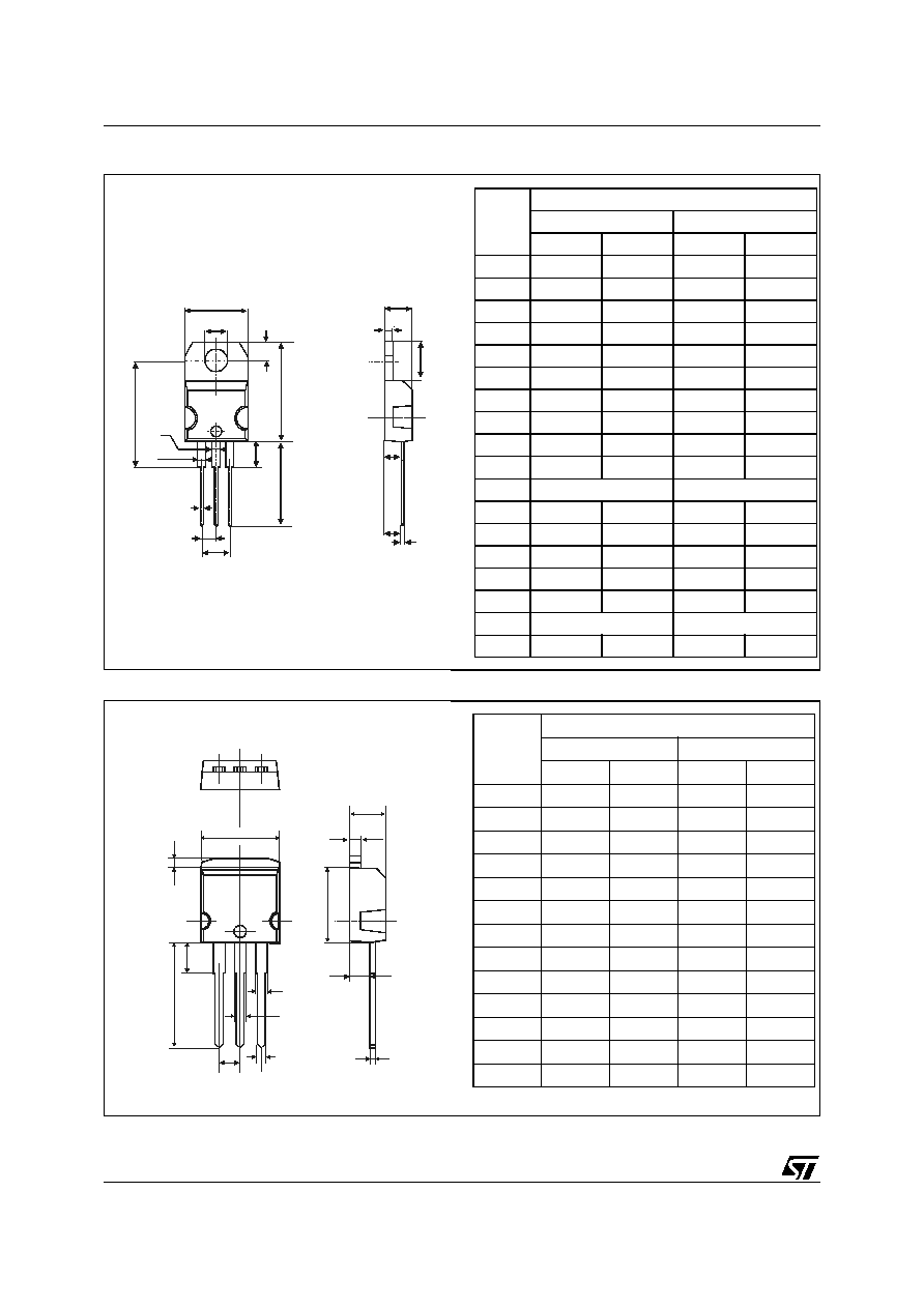
Figure 15: TO-220AB Package Mechanical Data
Figure 16: I
2
PAK Package Mechanical Data
A
C
D
L7
Dia
L5
L6
L9
L4
F
H2
G
G1
L2
F2
F1
E
M
e
D
L
L1
L2
b1
b
b2
E
A
c2
A1
c
REF.
DIMENSIONS
Millimeters
Inches
Min.
Max.
Min.
Max.
A
4.40
4.60
0.173
0.181
C
1.23
1.32
0.048
0.051
D
2.40
2.72
0.094
0.107
E
0.49
0.70
0.019
0.027
F
0.61
0.88
0.024
0.034
F1
1.14
1.70
0.044
0.066
F2
1.14
1.70
0.044
0.066
G
4.95
5.15
0.194
0.202
G1
2.40
2.70
0.094
0.106
H2
10
10.40
0.393
0.409
L2
16.4 typ.
0.645 typ.
L4
13
14
0.511
0.551
L5
2.65
2.95
0.104
0.116
L6
15.25
15.75
0.600
0.620
L7
6.20
6.60
0.244
0.259
L9
3.50
3.93
0.137
0.154
M
2.6 typ.
0.102 typ.
Diam.
3.75
3.85
0.147
0.151
REF.
DIMENSIONS
Millimeters
Inches
Min.
Max.
Min.
Max.
A
4.40
4.60
0.173
0.181
A1
2.49
2.69
0.098
0.106
b
0.70
0.93
0.028
0.037
b1
1.14
1.70
0.044
0.067
b2
1.14
1.70
0.044
0.067
c
0.45
0.60
0.018
0.024
c2
1.23
1.36
0.048
0.054
D
8.95
9.35
0.352
0.368
e
2.40
2.70
0.094
0.106
E
10.0
10.4
0.394
0.409
L
13.1
13.6
0.516
0.535
L1
3.48
3.78
0.137
0.149
L2
1.27
1.40
0.050
0.055
STPS2045C
7/8
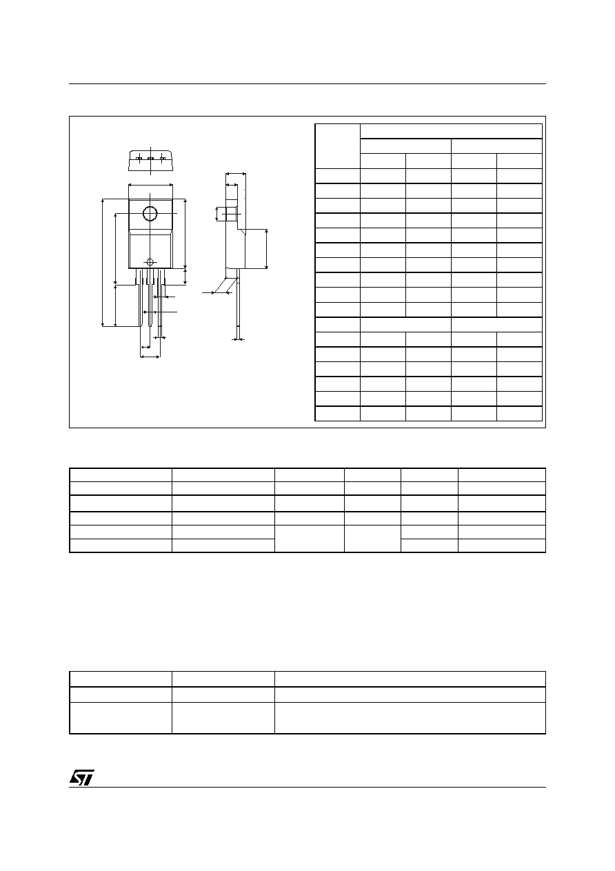
Figure 17: TO-220FPAB Package Mechanical Data
H
L3
L2
L4
L6
G
G1
F
F1
L5
D
E
L7
A
B
Dia
F2
Table 6: Ordering Information
Epoxy meets UL94, V0
Cooling method: by conduction (C)
Recommended torque value: 0.8 m.N.
Maximum torque value: 1.0 m.N.
Ordering type
Marking
Package
Weight
Base qty
Delivery mode
STPS2045CT
STPS2045CT
TO-220AB
2.23 g
50
Tube
STPS2045CR
STPS2045CR
I
2
PAK
1.49 g
50
Tube
STPS2045CFP
STPS2045CFP
TO-220FPAB
2.0 g
50
Tube
STPS2045CG
STPS2045CG
D
2
PAK
1.48 g
50
Tube
STPS2045CG-TR
STPS2045CG
1000
Tape & reel
Table 7: Revision History
Date
Revision
Description of Changes
05-Oct-2004
4F
Last update.
01-Dec-2004
5
Figure 16 (I
2
PAK Package Mechanical Data):
references b1 and b2 changed from 1.17mm to 1.70mm.
REF.
DIMENSIONS
Millimeters
Inches
Min.
Max.
Min.
Max.
A
4.4
4.6
0.173
0.181
B
2.5
2.7
0.098
0.106
D
2.5
2.75
0.098
0.108
E
0.45
0.70
0.018
0.027
F
0.75
1
0.030
0.039
F1
1.15
1.70
0.045
0.067
F2
1.15
1.70
0.045
0.067
G
4.95
5.20
0.195
0.205
G1
2.4
2.7
0.094
0.106
H
10
10.4
0.393
0.409
L2
16 Typ.
0.63 Typ.
L3
28.6
30.6
1.126
1.205
L4
9.8
10.6
0.386
0.417
L5
2.9
3.6
0.114
0.142
L6
15.9
16.4
0.626
0.646
L7
9.00
9.30
0.354
0.366
Dia.
3.00
3.20
0.118
0.126

STPS2045C
8/8
Information furnished is believed to be accurate and reliable. However, STMicroelectronics assumes no responsibility for the consequences
of use of such information nor for any infringement of patents or other rights of third parties which may result from its use. No license is granted
by implication or otherwise under any patent or patent rights of STMicroelectronics. Specifications mentioned in this publication are subject
to change without notice. This publication supersedes and replaces all information previously supplied. STMicroelectronics products are not
authorized for use as critical components in life support devices or systems without express written approval of STMicroelectronics.
The ST logo is a registered trademark of STMicroelectronics.
All other names are the property of their respective owners
© 2004 STMicroelectronics - All rights reserved
STMicroelectronics group of companies
Australia - Belgium - Brazil - Canada - China - Czech Republic - Finland - France - Germany - Hong Kong - India - Israel - Italy - Japan -
Malaysia - Malta - Morocco - Singapore - Spain - Sweden - Switzerland - United Kingdom - United States of America
www.st.com